CROWM
Overview • Description • References • Contact
Overview
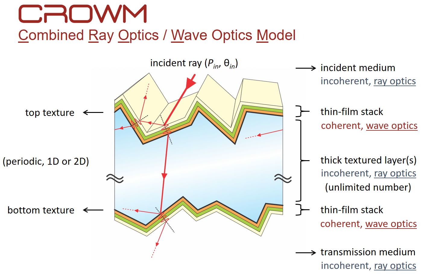
The optical simulator CROWM (Combined Ray Optics / Wave Optics Model) has been developed for optical simulation of multi-layered optoelectronic structures comprised of multiple thick (incoherent) and thin (coherent) layers (example structure). The thick layers can be either flat or textured; in the latter case, arbitrary 1D or 2D textures with lateral and vertical features in the range of micrometres or millimetres can be applied on either side of the layers (example textures).
The main input parameters of a typical CROWM simulation are the illumination conditions, the exact structure of the simulated device, and the optical properties of the materials used in the device. The main output parameters are the total reflectance and the total transmittance of the entire device, and the absorptances within each of the individual layers.
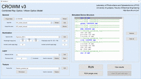
CROWM is equipped with a graphical user interface (GUI) which can be used for running the simulations, for viewing and editing the input files, for drawing the 3D schematics of the textures, and for the analysis and comparison of simulation results. Optionally, CROWM can also be run directly from the command line or even from within other programs such as Matlab.
Key features
- combined optical model (3D ray tracing + 1D transfer matrix formalism) for accurate analysis of incoherent and coherent light propagation
- simulation of flat and textured structures in three dimensions
- arbitrary 1D or 2D micro-scale textures can be included
- fully-featured graphical user interface, simple presentation of the results
- multi-core processing supported
- runs on 64bit Windows operating system
Additional features / Modules
- arbitrary angular intensity distribution of the incident illumination (e.g. Lambertian, etc.)
- extraction of the angular intensity distribution from an arbitrary thick layer in the structure
- volumetric scattering on particles embedded in a thick layer (e.g. phosphors)
- photoluminescence of particles embedded in a thick layer (e.g. phosphors)
- simulation of nano-textured interfaces using RCWA or other rigorous methods
- simulation of emission devices (e.g. OLEDs)
Resources
Description
General simulation structure
The optical simulator CROWM was primarily developed for complete optical analysis and optimisation of optoelectronic devices that consist of:
- One or more thick incoherent layers with the thickness in the range of 10 μm – 10 mm.
- Optional one-dimensional or two-dimensional surface textures applied to the top surface and/or the bottom surface of the thick incoherent layers. The textures at the top and bottom surface do not need to be the same. The lateral and vertical features of the textures are in the range of micrometres or larger. The textures are assumed to be periodic in both directions and should be continuous and single-valued everywhere (i.e. a single z value per (x,y) coordinate).
- An arbitrary number of thin films located in between the thick incoherent layers. The thicknesses of thin films should be in the range of 1 nm – 1 μm and are assumed to be much smaller than the lateral and vertical features of the textures. As a result, the thin films are assumed to be locally flat (parallel to each other and the surface of the thick layers).
- The incident medium (typically air) and the medium in transmission, which are assumed to be infinitely thick and thus incoherent.
Schematic of the general device structure that can be simulated in CROWM.
Optical model
CROWM combines two numerical approaches for the optical analysis of the thick and thin components of the simulated structure:
- Light propagation through the incident medium, the thick surface-textured layers, and the medium in transmission is analysed by means of incoherent three-dimensional ray tracing based on geometric optics. The incident illumination, which can be applied under an arbitrary incident angle (combination of azimuth and zenith angles), is divided into a number of rays which are then traced through the structure. The intensities and the directions of the rays are determined by the texture morphology (refraction and reflection effects at the interfaces), the optical absorption in the material (in the case of absorptive layers), and the calculated reflectances and transmittances through the thin-film components (calculated with a different model; see below). The textures are assumed to be periodic, in which case the boundary conditions are applied to the lateral borders of the ray tracing domain (i.e. a ray reaching the left border will reappear at the right border, and vice-versa).
- The thin-film stacks in the simulated structure are treated by means of fully-coherent transfer matrix formalism, which is a widely established one-dimensional method for simulation of light propagation through a stack of thin layers, taking into account coherence effects such as destructive and constructive interference. The thin-film stacks are assumed to be parallel to each other (i.e. the textures of the thick layers are transferred to all the interfaces within the thin-film stacks).
Areas of application / References
Silicon solar cells
Optimization of textured back contacts in silicon solar cells:
- Z. Holman, M Filipič, B. Lipovšek, S. De Wolf, F. Smole, M. Topič, C. Ballif, “Parasitic absorption in the rear reflector of a silicon solar cell: simulation and measurement of the sub-bandgap reflectance for common dielectric/metal reflectors,” Solar Energy Materials and Solar Cells, vol. 120 (2014) pp. 426-430 (link)
- Z. Holman, M. Filipič, A. Descoeudres, S. De Wolf, F. Smole, M. Topič, C. Ballif, “Infrared light management in high-efficiency silicon heterojunction and rear-passivated solar cells,” Journal of Applied Physics, vol. 113 (2013) pp. 1-13 (link)
Optimization of bifacial silicon solar cells:
- A. Čampa, A. Valla, K. Brecl, F. Smole, D. Munoz, M. Topič, “Multiscale modeling and back contact design of bifacial silicon heterojunction solar cells,” IEEE Journal of Photovoltaics, vol. 8 (2018), pp. 89-95 (link)
Perovskite solar cells and perovskite-based tandem devices
Light management in perovskite solar cells:
- B. Lipovšek, J. Krč, M. Topič, “Microtextured light-management foils and their optimization for planar organic and perovskite solar cells”, IEEE Journal of Photovoltaics, vol. 8 (2018), pp. 783-792 (link)
- M. Jošt, S. Albrecht, L. Kegelmann, C. M. Wolff, F. Lang, B. Lipovšek, J. Krč, L. Korte, D. Neher, B. Rech, M. Topič, “Efficient light management by textured nanoimprinted layers for perovskite solar cells,” ACS Photonics, vol. 4 (2017), pp. 1232-1239 (link)
Light management in perovskite/silicon tandem solar cells:
- M. Jošt, E. Köhnen, A. B. Morales-Vilches, B. Lipovšek, K. Jäger, B. Macco, A. Al-Ashouri, J. Krč, L. Korte, B. Rech, R. Schlatmann, M. Topič, B. Stannowski, S. Albrecht, “Textured interfaces in monolithic perovskite/silicon tandem solar cells: advanced light management for improved efficiency and energy yield,” Energy & Environmental Science, vol. 11 (2018), p. 3511 (link)
- M. Jošt, S. Albrecht, B. Lipovšek, J. Krč, L. Korte, B. Rech, M. Topič, “Optimizing textured perovskite / silicon-heterojunction tandem solar cells,” E-MRS Spring Meeting 2016, Lille, France, 2-6 May (2016), pp. 1-6
- M. Filipič, P. Löper, B. Niesen, S. De Wolf, J. Krč, C. Ballif, M. Topič, “CH3NH3PbI3 perovskite / silicon tandem solar cells: characterization based optical simulations,” Optics Express, vol. 23 (2015), pp. A263-A278 (link)
Organic solar cells
Light management in organic solar cells:
- B. Lipovšek, A. Čampa, F. Guo, C. J. Brabec, K. Forberich, J. Krč, M. Topič, “Detailed optical modelling and light-management of thin-film organic solar cells with consideration of small-area effects,” Optics Express, vol. 25 (2017), pp. A176-A190 (link)
- B. Lipovšek, J. Krč, M. Topič, “Optimization of microtextured light-management films for enhanced light trapping in organic solar cells under perpendicular and oblique illumination conditions,” IEEE Journal of Photovoltaics, vol. 4 (2014) pp. 639-646 (link)
Thin-film silicon solar cells
Light management in thin-film silicon solar cells:
- B. Lipovšek, J. Krč, M. Topič, “Design and optimisation of thin-film silicon PV modules with surface-textured front glass by using a combined geometric optics / wave optics model,” 27th European Photovoltaic Solar Energy Conference and Exhibition, Frankfurt, Germany, 24-28 September (2012) pp. 2604-2607 (link) (poster – best visual presentation award)
- B. Lipovšek, J. Krč, M. Topič, “Optical model for thin-film photovoltaic devices with large surface textures at the front side,” Informacije MIDEM, vol. 41 (2011) pp. 264-271 (link)
Luminescent down-shifting layers
Development of an optical model for volumetric scattering and photoluminescence:
- B. Lipovšek, A. Solodovnyk, K. Forberich, E. Stern, J. Krč, C. J. Brabec, M. Topič, “Optical model for simulation and optimization of luminescent down-shifting layers filled with phosphor particles for photovoltaics,” Optics Express, vol. 23 (2015), pp. A882-A895 (link)
Method for determination of the n&k parameters of phosphor particles:
- A. Solodovnyk, D. Riedel, B. Lipovšek, A. Osvet, J. Gast, E. Stern, K. Forberich, M. Batentschuk, J. Krč, M. Topič, C. J. Brabec, “Determination of the complex refractive index of powder phosphors,” Optical Materials Express, vol. 7 (2017), pp. 2943-2954 (link)
Optimization of phosphor-based luminescent down-shifting layers:
- A. Solodovnyk, B. Lipovšek, D. Riedel, K. Forberich, E. Stern, M. Batentschuk, J. Krč, M. Topič, C. J. Brabec, “Key parameters of efficient phosphor-filled luminescent down-shifting layers for photovoltaics,” Journal of Optics (2017) (link)
- A. Solodovnyk, K. Forberich, E. Stern, J. Krč, M. Topič, M. Batentschuk, B. Lipovšek, C. J. Brabec, “Highly transmissive luminescent down-shifting layers filled with phosphor particles for photovoltaics,” Optical Meterials Express, vol. 5 (2015), pp. 1296-1305 (link)
Light emitting diodes
Light management in organic light emitting diodes:
- M. Kovačič, P.-A. Will, B. Lipovšek, M. Topič, S. Lenk, S. Reineke, J. Krč, “Coupled optical modeling for optimization of organic light-emitting diodes with external outcoupling structures”, ACS Photonics, vol. 5 (2017) pp. 1-9 (link)
- M. Kovačič, P.-A. Will, B. Lipovšek, J. Krč, S. Lenk, S. Reineke, M. Topič, “Combined optical model for micro-structured organic light-emitting diodes,” Informacije MIDEM, vol. 46 (2016), pp. 267-275 (link)
- J. Krč, B. Lipovšek, M. Topič, “Design for high out-coupling efficiency of white OLED using CROWM – a combined geometric/wave optics model,” Renewable Energy and the Environment – Solid State and Organic Lighting Meeting, Tucson, Arizona, 2-7 November (2013) (poster)
Contact
This simulator can be licensed. Information about licensing are available on request.
For additional information please contact:
- Benjamin Lipovšek, e-mail: benjamin.lipovsek@fe.uni-lj.si, tel.: +386 1 4768 845