^
Introduction
The main objectives of research in photovoltaics are to increase conversion efficiency of solar cells and reduce manufacturing costs. Production of solar cells consumes time and material, consequently the numerical modeling and simulation of the operation is indispensable in finding the optimum material and geometrical parameters of the solar cells. Models of solar cells are based on the theoretical and experimental results of a variety of fields for example solid state physics, statistical mechanics, quantum mechanics and chemistry. The aim of modeling is to develop a model that includes physical background of cells, while being sufficiently simple to allow rapid calculation. Today we use numerical methods implemented in software simulators to solve the equations of the model. With the solution of a system of equations we can determine the output characteristics of the cells.
With different measurements of solar cells we obtain material and geometric parameters that are used for numerical validation of the model and simulation of the output characteristics of solar cells, such as current-voltage characteristics and quantum efficiency. Important results of the simulations include open circuit voltage, short circuit current density, fill factor and conversion efficiency of solar cells. The analysis can determine which set of parameters gives the desired output characteristics of solar cells.
^
Electrical modeling of solar cells

In LPVO we have developed a computer program ASPIN2 that enables us to calculate the characteristics of solar cells in one or two dimensions. ASPIN2 is based on a verified drift-diffusion model with added models of thermionic emission and quantum tunneling. ASPIN2 also allows the inclusion of material inhomogeneites of polycrystalline solar cells. To calculate the optical generation profile SunShine optical simulator is used.
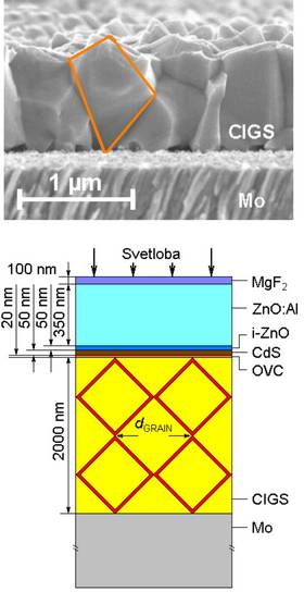
The figure shows a scanning electron microscope (SEM) scan of a CIGS solar cell (top). Based on the scan the simulated structure is determined (bottom). In describing the structure we take into account the inhomogeneities in the material due to the polycrystalline structure of the CIGS layer.
^
ASPIN2 example

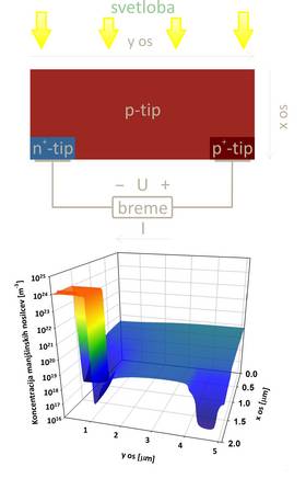
To demonstrate the use of ASPIN2 we simulated pn-solar cell with contacts on the back side. Light is incident upon the cell in the positive direction of x axis (Light enters the cell at x = 0). The material, which absorbs most incident light is p-type. In the lower left corner the material is n-type and the pn-junction is formed. In the lower right side heavily doped p-type creates back surface field. The figure shows simulated structure (top) and simulation results showing the concentration of minority charge carriers, in this case the electrons (bottom).
^
Contacts
For additional information please contact:
- Franc Smole, e-mail: franc.smole@fe.uni-lj.si, phone: +386 1 4768 330


